PATENT JP.7527588.B | A Method and a Device for Assembly of a Nanomaterial Structure
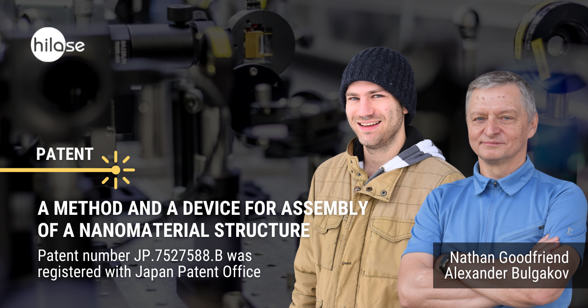
Nathan Goodfriend and Alexander V. Bulgakov from the Scientific Laser Applications department achieved a new patent for the HiLASE Centre, titled A Method and a Device for Assembly of a Nanomaterial Structure. On the 26th of July 2024, it was registered with Japan Patent Office, as patent no. JP.7527588.B.
This device and method was already patented with the United States Patent and Trademark Office (USPTO) last year.
The present invention relates to a method and device capable to form a nanomaterial structure on a receiver by transfer of nanomaterial from a donor film using the lase-induced forward transfer technique, preferably by blister-based laser-induced forward transfer. The method further comprises a simultaneous scanning of the donor film and/or the receiver so that, a computer driven means for moving the receiver and the donor film can form high precision nanomaterial structures.
The method and associated device (which you can view in the video below) will enable HiLASE Centre researchers to create complex nanotechnological structures at the atomic scale.