Researchers from the HiLASE Centre have contributed to a new paper published in the Frontiers in Nanotechnology journal. Among the co-authors are HiLASIANS from different teams and departments: Inam Mirza (Team Leader: Pulsed Laser Deposition), Alexander V. Bulgakov (Team Leader: Nanomaterials), Hana Turčičová (Senior Researcher: Harmonaics generation), Ondřej Novák (Team Leader: Non-linear optics), Jiří Mužík (Team Leader: Thin-disk lasers), Martin Smrž (head of Advanced Laser Development), Tomáš Mocek (head of HiLASE Centre) a Nadezhda M. Bulgakova (head of Scientific Laser Applications).
Other institutions represented in the team of authors of the paper titled Non-thermal regimes of laser annealing of semiconductor nanostructures: crystallization without melting include home institutions University of Pardubice and Brno University of Technology (Hanna Sopha, Jan M. Macak), as well as international Kutateladze Institute of Thermophysics, Novosibirsk State University and Rzhanov Institute of Semiconductor Physics (Sergey V. Starinskiy, Vladimir A. Volodin).
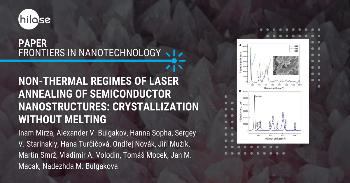
As-prepared nanostructured semiconductor materials are usually found in an amorphous form, which needs to be converted into a crystalline one for improving electronic properties and achieving enhanced application functionalities. The most utilized method is thermal annealing in a furnace, which however is time- and energy-consuming and not applicable for low-temperature melting substrates. An alternative is laser annealing, which can be carried out in a relatively short time and, additionally, offers the possibility of annealing localized areas. However, laser-annealed nanostructures are often distorted by melting, while preserving the as-prepared morphology is essential for practical applications. In this work, we analyze conditions of non-thermal ultrafast laser annealing of two kinds of nanostructures: anodic TiO2 nanotube layers and Ge/Si multilayer stacks. For both cases, regimes of crystallization have been found, which yield in preserving the initial nanomaterial morphologies without any melting signs. On these examples, ultrafast non-thermal mechanisms of structural material transformation are discussed, which can provide new opportunities for conversion of amorphous semiconductor nanomaterials into a desired crystalline form that is of high demand for existing and emerging technologies.