Functional surfaces may get a ‘new kick’ with the Direct Laser Interference Patterning (DLIP) technology developed at HiLASE.
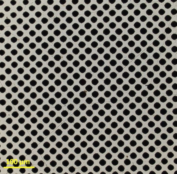
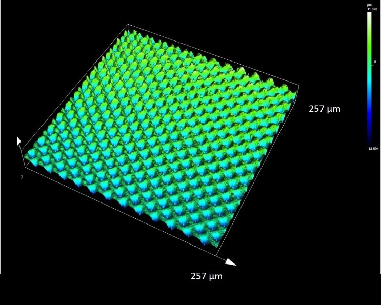
Fabrication of functional surfaces with micro and nanostructures for applications such as diffraction patterns to label goods (provenance protection), reduce surface friction, ensure superhydrophobicity or provide self-cleaning or antimicrobial properties are of great industrial interest.
Standard methods such as laser direct writing has shown a great potential to design surface structures, but at the cost of extensive processing times in the range of minutes per square centimetre. At HiLASE we deployed the four beam DLIP with PERLA high-intensity ultrashort pulsed lasers, which allows us to upscale the fabrication micro- and nano-structures of large surface areas and increase the fabrication speed in orders of magnitude.
That enables us to process an area of several millimetres in diameter with micron or sub-micron resolution.
If you want to know more about our DLIP capability please come visit us at SPIE Photonics West San Francisco, booth #3485, Hall E in the Moscone Center on the 4-6 Feb 2020.